p-e07-11a-sun 6 / 94
10秒後にBOOKのページに移動します
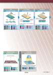
CVD Laser Milling Sputtering 4 p-i-n Layer Formation 5 p-i-n Layer Patterning 6 Backside Electrode Formation 13 Inspection Performance Test Module Transfer 12 Module Transfer Inspection Plasma p-Layer p-Layer i-Layer i-Layer n-Layer n-Layer Transparent electrode Laser Metallic backside electrode Laser Plasma is applied to form each layer. A laser is used to cut p-i-n layers to form circuits. Forms the metallic backside electrode. Tests output performance under artificial sunlight Transfers the modules. and checks pressure resistance and insulation. P.4 P.9 P.10 P.7 P.9 P.10 P.13 P.4 P.10 P.9 P.13 P.4 P.6 P.5 P.7 P.2 P.5 P.9 P.11 P.4 P.7 P.10 P.10 P.13 P.13 P.2 P.5 P.9 P.11 P.4 P.7 P.10 P.13 Vacuum-lift and transfer 1 Clean 1 Clean 3 Temperature control 3 Temperature control 3 Temperature control 7 Low vacuum 7 Low vacuum 7 Low vacuum 7 Low vacuum 10 High vacuum 10 High vacuum 2 Actuators 2 Actuators 2 Actuators 2 Actuators 2 Actuators 4 Heat resistant 8 Static electricity 6 Non-contact transfer 12 Sensors (Detection) 12 Sensors (Detection) 9 Reduced wiring 9 Reduced wiring 9 Reduced wiring 9 Reduced wiring 9 Reduced wiring 12 Sensors (Detection) 12 Sensors (Detection) 12 Sensors (Detection) 5 Corrosion resistant 5 Corrosion resistant 5 Corrosion resistant 5 Corrosion resistant Front matter 4